RDMA from Xilinx FPGA to Nvidia GPUs — Part 1
I have recently had the need to design a system concept able to process real-time video at a very high frame rate on a desktop PC.
The algorithm required to implement was partially suitable for GPUs and partially suitable for FPGAs where in this case the video interface, capture and the main algorithmic function were suitable for an FPGA but the algorithmic pre-processing was found suitable for a GPU.
My design recommendation was a heterogeneous Intel CPU PC based computing system consisting of a Xilinx FPGA and an Nvidia GPU connected over PCIe.
In order to keep the frame rate high and the latency as low as possible, I have decided to use Nvidia’s Remote Direct Memory Access (GPUDirect RDMA). This feature enables remote PCIe endpoints to bypass the need to use the Host CPU’s memory, which then requires a second memory copy to the GPU, by allowing the endpoint to write directly to the GPU’s memory.
The setup I used for testing is:
- Intel Xeon running Ubuntu 18.04LTS
- Xilinx KCU105 PCIe Evaluation Board
- NVidia P2000 and later NVidia RTX6000
While I’m not a software developer, I do have some programming background and previous Linux kernel driver programming experience. That being said, my code was probably not written using good coding practices but it was written with the sole intention of testing the hardware… and hey… it works.
This is Part 1 of the post and it will only briefly describe the concept, design and results while giving some (hopefully) helpful links. Part 2 of the post will go futhur into the FPGA and Kernel Driver code.
The FPGA design
The heart of the Vivado design is an AXI Bridge for PCIe Gen3 Subsystem IP configured to have 1 BAR and 1 PCIe outbound translation. This block converts inbound AXI transactions to outbound PCIe transactions and inbound PCIe transactions to outbound AXI transactions.
In order to generate the AXI write transactions to the PCIe block I like to use the AXI Datamover IP. This IP receives a command via an AXI Stream interface (basically only data and valid) and the data stream itself via a second AXI Stream interface leaving the IP to handle all the little AXI write quirks.
The last main block in the design is the main state machine block which generates the write commands as configured using its register block. This block has two modes, one mode is used to write a single 32bit word to the PCIe and wait for an acknowledge write command from the PCIe measuring the round trip time back and forth to the PCIe endpoint (the GPU in this case). The second mode is a video pattern simulation written to the PCIe endpoint configurable to different frame sizes and frame rates which is intended for stress testing the GPU interface.
The Linux Kernel Driver
For this experiment I have found the following sources useful and would like to thank and credit their authors:
- Bluespec PCIe library
https://github.com/sangwoojun/bluespecpcie/blob/master/distribute/driver/bdbmpcie.c
This link contains a nice example of a PCIe driver source code for a Xilinx FPGA - GPUDirect RDMA example
https://github.com/karakozov/gpudma
This link contains the best example I found online for an RDMA driver - Developing a Linux Kernel Module using GPUDirect RDMA
https://docs.nvidia.com/cuda/gpudirect-rdma/index.html
This link contains the formal RDMA driver documentation from Nvidia
Without going into too much details, the Kernel driver has three main functions. The first function is to serve as the FPGA PCIe Driver — setup the interrupts and BAR mapping. The second function is to allocate and pin pages in GPU memory using nvidia_p2p_get_pages() function which allows this memory region to be accessed directly from an external PCIe device. The third and last function of the Kernel driver is to return the pinned memory physical address to the FPGA in order for it to be able to write to this address via PCIe.
As mentioned before Part 2 of the post will go futher into the FPGA and Kernel Driver code details. For now, I hope the links provided can give you a jumpstart…
The GPU CUDA Kernel
The GPU CUDA Kernel is really not affected by the RDMA implementation. The Kernel receives a pointer to the pinned GPU memory and runs as needed. The only piece worth mentioning, in my opinion, is the option to map a region in the host’s physical address to be accessed directly by the GPU. I found this useful to create an IPC/Mailbox between the GPU and FPGA.
I used a simple method (and surely not best practice). First, the host used mmap() “ /dev/mem” at the FPGA PCIe BAR address offset (0xb5c00000 in my example… Yes i know… i used a static address and it should be dynamically given by the PCIe driver but remember: “it was written with the sole intention of testing the hardware”) with the size of the BAR registers to get a virtual address of the FPGA BAR that can be accessed by the Host.
fd_fpga = open(“/dev/mem”, O_RDWR|O_SYNC);
fpga_reg = (int *)mmap(0, 0x10000, PROT_READ|PROT_WRITE, MAP_SHARED, fd_fpga, 0xb5c00000);
After that, the CUDA code received the pointer to the mapped virtual address and used two functions, one to register the host memory address and a second to receive a pointer that can be directly used by the CUDA Kernel running on the GPU.
checkCudaErrors(cudaHostRegister(fpga_reg, 0x10000, cudaHostRegisterIoMemory));
checkCudaErrors(cudaHostGetDevicePointer((void **)&d_fpga_reg, (void *)fpga_reg, 0));
I used this method to have the GPU directly write to the FPGA when certain events occurred i.e. when the first data word arrived, the last data word arrived or when the GPU processing has completed.
The Basic Measurements
Using the building blocks described above, I implemented a system in which the FPGA writes a video frame directly to the GPU memory, the GPU would indicate to the FPGA when the first data word has arrived, the last data word arrived, preform some sort of data manipulation on the data and indicate when the GPU processing has completed.
The FPGA implemented multiple counters counting from the point the first image pixel started transmission to the PCIe until the various GPU indications have arrived. The FPGA also implemented a time histogram logic to preform statistical analysis of the measured latency distribution.
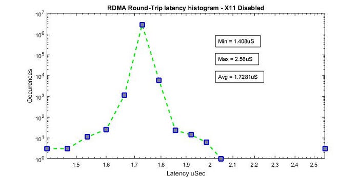
On the initial measurements I got the following results for the RDMA latency for the first pixel written to the GPU (Round-Trip because it measures both the time it took the pixel to be written to the GPU and the time it took the GPU to write the indication back to the FPGA):

While these results were pretty good on average @ 1.73uSec, you can see that some of the transactions took too long to occur and this was unacceptable for a “real-time” system.
It took me some time to remember that I only had a single GPU installed and that it was also being used by the X11 window driver (Ubuntu’s graphical interface).
I used systemctl set-default multi-user.target to disable the graphical interface after Linux startup (Again… maybe there is a better way but “it was written with the sole intention of testing the hardware”) and repeated the above measurements with the following results:

These results were much better and allowed me to proceed with the proof of concept for this design.
Conclusion
In Part 1 I showed a brief introduction to an RDMA concept for a very high frame rate processing system able to transmit video frames between a Xilinx FPGA and an Nvidia GPU with an extremely low latency @ 1.73uSec.
In Part 2 I will try to go into the code itself…
I hope you found this somewhat helpful.


